Designing the ISA and the simulator is fine and dandy but it does not beat running a custom CPU on real hardware. Unfortunately, I don't have tens of thousands of euros to make a custom chip. The best I can do is to run it on an FPGA. An FPGA is a chip with a lot of logic gates that can be wired together to make any logic circuit. And our CPU is a logic circuit.
What we need to do is to use a hardware description language such as Verilog or VHDL to describe the CPU. I choose to use Verilog as I prefer its more concise syntax but both languages can do the same things in a very similar manner.
I designed my CPU in 4 main blocks:
The CPU is nice to have but it cannot do much on its own. It needs peripherals to interact with the outside world. The one we will use the most is the UART, a peripheral used to send and receive serial messages, such as our beloved "Hello, world!"
The peripherals are put on the memory bus of the CPU so that they can be interacted with. There is also the RAM and the ROM of the processor on that bus.
The peripherals are controlled by writing and reading at special memory addresses, in a way similar to the simulator. For example, the addresses used to interact with the UART are between 0xFF16 and 0xFF19. Here is the code used to do so, notice how similar it is to the code that ran on the simulator:
@align_word
label string
@string Hello, world!
@rawbytes D A 0

label start
    set 15
    cpy R3 ; Length of the message to print in R3
    setlab string
    cpy R2 ; Pointer to the character to print in R2
    label print-loop
        ; Loading a character from R2 and storing it in R3
        tbm
        load R2
        cpy R1
        tbm
        ; Function call made thanks to the `callf` macro
        callf printc
        ; Incrementing the pointer to the desired character
        set 1
        add R2
        cpy R2
        ; Decrementing the number of characters left to print
        set 1
        sub R3
        cc2
        cpy R3
        ; If the number of characters left to print is not 0, jump back to the start of the loop
        set 0
        eq R3
        cmpnot
        setlab print-loop
        jif
    quit

label printc
    pushr R2 ;addrs
    pushr R4 ;waiting loop pointer
    set+ 0xFF16 ;UART tx_cmd addr
    tbm
    cpy R2
    setlab printcLoop
    cpy R4
    label printcLoop
        load R2 ;testing that R2 is not 0 to see if we are ready to print
        cpy R12
        set 0
        eq R12
        read R4 ;until ready, go back
        jif
    set 1    ;computing the data addr
    add R2
    cpy R12
    read R1 ;writing the char
    str R12
    set 0   ;sending command
    str R2
    tbm
    popr R4 ;restoring registers
    popr R2
    ret
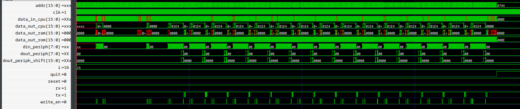
To ensure that everything works well, it is important to test the CPU, its code, and its peripherals. For example, here is the result of the simulation that sends "Hello, world!" over a UART TX line.
Note how the TX line moves a bit each time a character is sent.
Once the Verilog code is ready, we must synthesize it to convert it into a bitstream that can be loaded into the FPGA. Here comes the not-fun part: "Slack not met".
If a signal goes through too many logic gates between two registers, the signal does not have the time to be fully updated before reaching the end register. This causes the design implemented in the FPGA to have a different behavior than what has been described in Verilog. Thankfully, the FPGA design tools (Vivado in my case) can alert us if such a problem arises and it is up to the designer to fix the issue.
The issue can be fixed by putting intermediate registers in the signal paths that cause issues. This increases latency but this is a small price to pay to have a working design. Once the issues are ironed out, the design can be downloaded to the FPGA.
We are now able to have our hardware design in the FPGA, but how can we give it software to run? The first solution is to bake the software as a ROM in the MCU design. This is very easy to do but this has a major drawback, to put a new software, we must restart the synthesis process, which is lengthy.
A better solution is to embed a bootloader in the MCU that can read firmware given over the UART link and put it into memory. That way, new software can effortlessly be downloaded.
The bootloader is a normal program that I write into a ROM in the MCU. It is executed on boot and uses the peripherals (UART and timers) to get the desired software from an outside source and write it into RAM from which it will be executed. Once the software is fully loaded, the bootloader resets the MCU's state and jumps into the new software.
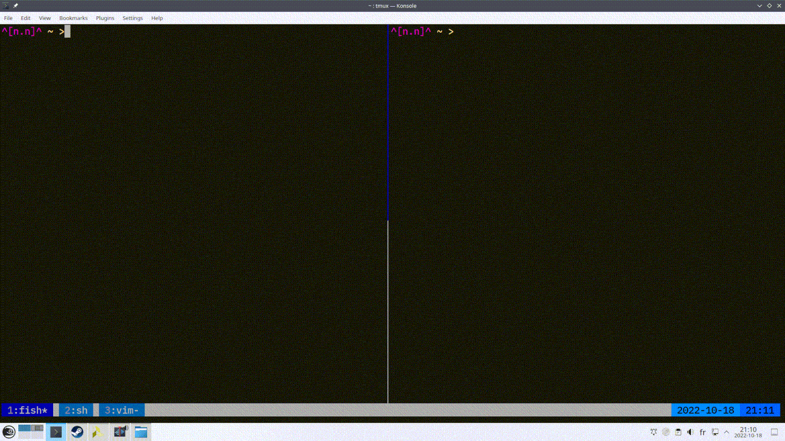
Here is a small clip of me uploading the "Hello, world!" program to the processor and its reply.
Sending a "Hello, world!" over a UART link is a nice step, but it would be even better to write it onto a screen. To do so, we will need to design a basic GPU to pair with our CPU.